Sustainable Circuits: Exploring Lead-Free PCB Assembly Techniques

In 2006, the European Union released the Restriction of Hazardous Substances (RoHS) legislation; after that, lead-free PCBs surpassed the demand for lead-containing PCBs, and in the whole world, the demand for lead-free PCB assembly is relatively high. However, in some regions like Africa,, Southeast Asia, and South Asia, there is still a slight demand for lead-containing PCBs while the demand for lead-free PCBs is becoming universal. In the regions like America, Europe, the Middle East, and Australia, the assembly of PCB must be lead-free.
The assembly of the printed circuit boards (PCBs) without using lead at any manufacturing phase is called lead-free assembly of PCBs. Lead is dangerous for humans as it is a poisonous substance. However, it was being used in the soldering process of the PCBs. However,, the manufacturing process of the PCBs remains almost the same, whether or not there is a use of lead. This article focuses on lead-free PCB assembly techniques, which are sustainable circuit production methods in our electronic world.

PCB Assembly
Lead-Free PCB Surface Finishes
The surface treatments for the lead-free assembly might be required, such as lead-free HAL, ENIG, OSP, immersion silver, gold plating, immersion tin, carbon ink, and ENEPIG. For the flexible PCBs, the use of lead-free HASL is unsuitable, but OSP or ENIG could be used as a substitute. Because OSP is effortlessly oxidized, the PCB maker must package the circuit boards panel by panel in vacuum bags if not assembled immediately after PCB fabrication. Unpacking the lead-free PCBs should only happen when positioned on the SMT lines. It is not possible to bake OSP PCBs before PCB assembly services. Additionally, be aware that OSP PCBs must be stored for 30 days. To reapply OSP, return the boards to the PCB manufacturer if the storage duration exceeds thirty days.
Excellent soldering characterizes ENIG and ENEPIG, which are utilized in high-reliability PCBAs.
Lead-Free Solder Paste
The characteristics of solder paste are critical in PCB assembly. Of course, we need to use lead-free solder paste in lead-free PCB assembly services. You can find the lead-free solder in the green bottles that follow up with the standards of RoHS. The usage temperature of the solder paste must be between 22 and 28 degrees Celsius. Meanwhile, the storage temperature must be between 2 and 8 degrees.
Lead-Free Components
Besides printed circuit boards; we need to ensure all the electronic components are lead-free, such as ICs, resistors, capacitors, transformers, connectors., etc. Also, all the support tools and equipment used in the lead-free PCB assembly line should be without lead.
Lead-free PCB Assembly
According to RoHSRoHS regulations, the lead concentration must be less than 0.1% in solder paste for assembly. The production line, entire manufacturing process, electronic devices, PCB boards, and solder paste should all be lead-free for the assembly to be considered lead-free.
The lead requirement in the manufacturing process in one-stop lead-free PCB assembly is Pb<0.1%. It comprises all the electronic components, PCB base laminates, surface treatment, PCB ink, solder paste, packing bags/boxes, housing, and all the other devices/fixtures and equipment in the assembly process. Moreover, lead-free solder paste, lead-free wave soldering, lead-free reflow soldering, and lead-free surface treatment are the essential components of the lead-free PCB assembly.
Steps Involved in the Assembly of Lead-free PCBs
For the PCB with lead-free assembly, assembly lines like SMT assembly and PTH assembly should also be lead-free. However, the PCB that has lead can also be assembled on lead-free assembly lines. However, the problem would arise that machines would get contaminated with lead and no longer be used again. So we must remember that all the materials, such as PCB bare boards and electronic components, and the whole PCB assembly process should be lead-free.
-
Solder Paste Printing
The lead-free solder paste is silk-screened on the PCB pads with the help of SMT stencil in the next step. Then, the paste inspection machine inspects whether the solder paste is suitable for the reflow soldering process in size and width. We can also use manual visual inspection for small-batch production.
-
Surface Mount Devices (SMD) Pick and Place
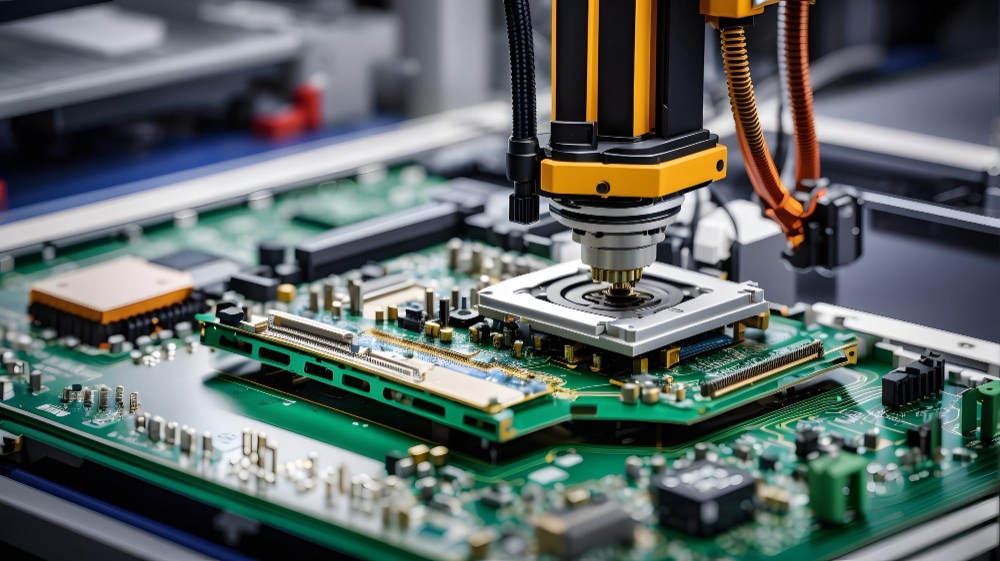
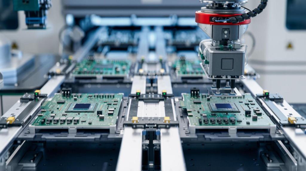
The critical process in PCB assembly is the pick and placement of SMD components because any minor mistake will cause serious problems. Automated pick and place equipment is used to get a good quality. The robot arm places the surface mount devices on the pads before the reflow soldering. AOI or manual visual inspections will be done to make sure the components are set correctly. First, article approval is critical to avoid considerable mistakes in mass production. The manufacturer may perform the x-ray inspection if BGA assemblies are on the circuit boards to ensure that solder balls are suitable for the reflow soldering.
-
Reflow Soldering Process
The PCBs with components will be run through a reflow soldering oven, and the PCBs will be warmed in different temperature zones before the soldering process. They make sure that the oven temperature matches the profile of reflow soldering to make the lead-free PCBs. The solder paste melts during the procedure, wetting the PCB pads. Then, the SMD components are soldered to the PCBs and removed from the oven for cooling.
We should know that lead-free solder paste’s paste’s lead-free soldering temperature is higher than leaded solder paste. For lead-free PCBs, the temperature ranges from 240 to 270 degrees Celsius. For the assembly of PCBs that use lead-free solder, the temperature is approximately 30 degrees higher. The following essential point is the soak, cooling stages, and warm-up in the lead-free reflow profile.
For PCBs that have thick copper, the temperature must be high. Because at low temperatures, the PCB pads would solder inappropriately. According to the experts, the maximum temperature could be between 290 and 300 degrees Celsius.

Lead-Free PCB Assembly
-
Automatic Optical Inspection (AOI)
If the PCB has the double-mounted components, then the PCB assembly would be returned to the assembly lines to be attached to the other side. Usually, nitrogen reflow soldering is considered if there are chances of oxidation of PCBA during the procedure. To make sure that there are no significant issues like missing parts or spaces, the manufacturer uses automatic optical inspection (AOI). Next, it is transferred to the PTH PCB assembly lines.
-
Wave Soldering Process
After inserting PTH component pins into the PTH holes, we run the PCBs through the wave soldering machine. The components will be dipped into a boiling liquid lead-free tin tank, and the pints will be soldered by tin when cooling down in order to get the required part exposed to the soldering wave, it is placed in a jig. For the prevention of thermal shocks, selective soldering is preferable to wave soldering. Then eventually, the THT pins are cleaned and examined and reduced to 1 to 2 mm in length.
-
Testing and Packaging
In the last step, there is testing and packaging of lead-free PCB assembly. IPC-600D testing guidelines are monitored for the PCBs. At this point, the solder junctions are inspected and tested. AOI and X-ray inspection come after visual examination. Testing is done both functionally and physically before packing.
Anti-electrostatic discharge bags are exceptionally vital for the packaging of lead-free PCBs. This is essential to promise that static charges won’t affect the finished product when transported.
Conclusion
In most of the world, lead-free is the essential and most common requirement for PCBs. You have to make sure that the manufacturer uses PCB assembly lines that are only lead-free for the assembly of lead-free PCBs. Also, make sure all the PCB bare boards, electronic parts, and other items are all lead free. However, Lead-free PCB assembly is a complex process that should only be carried out by experienced manufacturers.

Don't Buy an iPhone Air Case Without Knowing the Returns Policy

How Federal Assistance Programs Now Support More Than Their Original Purpose

How Email Widgets Can Support Time-Sensitive Email Marketing


