High frequency PCB manufacturing is one of the most demanding areas of PCB production. Boards designed to operate at frequencies above 500 MHz, and often well into the GHz range, behave differently from standard digital boards. At these frequencies, the electrical properties of the laminate material, the geometry of every trace, the via structures, and the grounding arrangement all directly affect whether the board transmits signals cleanly or introduces loss, noise, and reflected energy that degrades system performance.
Standard FR4, the material used in most multilayer PCBs, is not suitable for high frequency applications above around 1 GHz. Its dielectric constant varies with frequency, its dissipation factor is too high, and its copper surface roughness adds significant insertion loss at microwave frequencies. High frequency PCB manufacturing uses a different set of materials, tighter process controls, and different design rules to solve these problems.
This article covers the materials used in high frequency PCB production, the manufacturing tolerances that matter most, the design practices that separate working RF boards from boards that need multiple revision cycles, and what to look for in a manufacturing partner.
What High Frequency PCB Manufacturing Involves
A high frequency PCB is a printed circuit board designed to carry signals in the RF and microwave frequency range. This typically means above 500 MHz, though the specific threshold where standard FR4 becomes a problem depends on the loss budget of the design. Some designs operating at 1 to 2 GHz can tolerate FR4 if insertion loss margins are generous. Designs at 5 GHz and above almost always require specialty laminates.
The defining challenge of high frequency PCB design is maintaining signal integrity across the board. At microwave frequencies, energy does not simply flow through copper traces the way it does at DC or low frequencies. The signal travels as an electromagnetic wave guided by the trace and its reference plane. The dielectric material between the trace and the reference plane, the geometry of the trace, and the electrical properties of the laminate all determine how well that wave is guided and how much energy is lost or reflected along the way.
High frequency PCB manufacturing addresses this challenge by using laminate materials with stable, low dielectric constants and low dissipation factors, controlling trace geometry to tight tolerances, managing copper surface roughness, and applying quality control processes that verify electrical performance rather than just visual appearance.
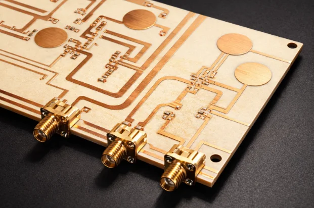
FastTurn PCB specializes in high frequency PCB manufacturing using Rogers, Taconic, Isola, and PTFE-based laminates. Their production supports trace widths and spacing down to 3 mil, drilled holes as small as 0.15 mm, controlled impedance to within plus or minus 5 ohms, and board thickness from 0.2 mm to 3.2 mm. Lead times start at 2 to 3 days for urgent prototype builds.
Why Standard FR4 Does Not Work at High Frequencies
FR4 is a glass-fiber-reinforced epoxy laminate that performs well for digital circuits operating below about 1 GHz. Above that frequency, several properties of FR4 become problems.
Dielectric constant variation
The dielectric constant of FR4, often listed as approximately 4.5, is not stable across frequency. It shifts as frequency increases. For a controlled impedance trace, the characteristic impedance is calculated based on the dielectric constant of the material. If the dielectric constant changes with frequency, the impedance of the trace changes too, creating a mismatch between the source, the trace, and the load. This mismatch causes signal reflection, which degrades both signal integrity and return loss.
High frequency laminates like Rogers RO4003C have a dielectric constant of 3.55 that is stable to within 0.05 from 500 MHz to 10 GHz. Taconic TLY and RF laminates based on PTFE have Dk values as low as 2.2 with similar stability. This consistency makes controlled impedance predictable and reliable.
Dissipation factor
The dissipation factor, also called the loss tangent, measures how much energy the dielectric absorbs and converts to heat as a signal passes through it. Standard FR4 has a dissipation factor around 0.020 at 1 GHz. Rogers RO4003C has a dissipation factor of 0.0027. That is roughly seven times lower.
At 1 GHz on a short trace, the difference may be acceptable. At 10 GHz on a 10 cm trace, the difference in insertion loss is significant. In amplifier chains, filter designs, and antenna feed networks where loss directly affects gain, noise figure, and efficiency, using the wrong laminate material can make the difference between a design that meets specification and one that does not.
Copper surface roughness
At high frequencies, the current in a copper trace concentrates near the surface of the conductor. This is called the skin effect. As frequency increases, the skin depth decreases. At 10 GHz, the current flows in a layer only about 0.66 micrometers thick on the surface of the copper.
The surface of standard rolled and annealed copper foil is rough at the microscopic level. The signal traveling along that rough surface must follow a longer actual path than a perfectly smooth surface would provide. This extra path length increases conductor loss. High frequency laminates are often paired with very low profile copper foil, which has a smoother surface and lower conductor loss at microwave frequencies. FastTurn PCB uses low profile copper foil with their high frequency laminates to minimize skin effect losses.
High Frequency Laminate Options
Choosing the right laminate is the first and most important decision in high frequency PCB design. FastTurn PCB works with a range of high frequency materials, and the right choice depends on your frequency range, loss budget, thermal environment, and cost targets.
Rogers RO4000 series
Rogers RO4003C and RO4350B are the most widely used high frequency laminates for commercial and industrial RF applications. RO4003C has a Dk of 3.55 and a dissipation factor of 0.0027 at 10 GHz. RO4350B has a Dk of 3.66 and a dissipation factor of 0.0037 at 10 GHz. Both materials are glass-fiber reinforced, which gives them better dimensional stability and easier processing than pure PTFE laminates. They can be drilled, routed, and handled with standard PCB fabrication equipment, making them practical for volume production and fast turn prototyping.
RO4000 series materials are used extensively in 5G antenna elements, automotive radar, LTE base station filters, point-to-point microwave links, and satellite communication ground terminals. FastTurn PCB carries RO4003C and RO4350B in stock and can produce prototype builds in 2 to 3 days when Gerber files are ready.
Rogers RO3000 series
RO3003, RO3006, and RO3010 are PTFE-based laminates with ceramic filler, offering lower Dk values than the RO4000 series. RO3003 has a Dk of 3.00, RO3006 a Dk of 6.15, and RO3010 a Dk of 10.2. The higher Dk options reduce the physical dimensions of quarter-wave transmission lines and resonators, which is useful for compact filter and antenna designs at 5 GHz and above. These materials require plasma treatment for hole wall preparation before plating, which FastTurn PCB performs with dedicated PLASMA processing equipment.
Taconic laminates
Taconic produces a range of PTFE and PTFE-glass laminates including the TLY, RF, and TSM families. Taconic TLY has a Dk of 2.2, the lowest available in a woven-glass PTFE laminate. This very low Dk produces wider traces for a given impedance target, which reduces conductor loss. Taconic RF materials are used in demanding microwave and millimeter-wave applications. FastTurn PCB works with Taconic laminates for designs that require properties outside the Rogers product range.
Isola laminates
Isola produces materials such as I-Tera MT40 and Atera, which are glass-reinforced laminates targeting the high-speed digital and RF market. These materials have lower Dk and Df than standard FR4 but are glass-reinforced and process similarly. They are often used in mixed-signal boards where some layers carry high-frequency RF signals and other layers carry digital signals, allowing the use of specialty laminates on RF layers and more economical materials on digital layers.
PTFE-only laminates
Pure PTFE laminates without glass fiber reinforcement, such as those from Arlon and 3M, offer the lowest possible Dk values and excellent dissipation factors for millimeter-wave applications above 30 GHz. They are mechanically softer and more difficult to process than glass-reinforced materials, requiring specialized drilling parameters, plasma desmear, and careful handling. FastTurn PCB uses dedicated equipment including PLASMA processing systems for PTFE hole wall preparation on these demanding materials.
Manufacturing Tolerances That Matter in High Frequency PCB Production
High frequency PCB performance is highly sensitive to dimensional variation. The tolerances that matter most are those that directly affect controlled impedance, insertion loss, and return loss.
Trace width tolerance
Characteristic impedance on a microstrip or stripline trace is a function of trace width, dielectric thickness, copper weight, and Dk. A 1 mil variation in trace width on a 50 ohm microstrip trace built on RO4003C produces roughly a 2 to 3 ohm shift in impedance depending on the trace geometry. FastTurn PCB holds trace width to within plus or minus 0.5 mil on high frequency builds using their LDI imaging and controlled etching process. This tolerance keeps impedance variation within the plus or minus 5 ohm target for most designs.
Dielectric thickness tolerance
The thickness of the dielectric between a signal trace and its reference plane directly determines trace impedance. Variation in dielectric thickness causes variation in impedance along the length of a trace. High frequency laminates have tighter Dk and thickness tolerances than standard FR4 prepreg, which is one of the reasons they cost more. FastTurn PCB uses premium laminate materials with controlled thickness specifications and applies lamination process controls to maintain dielectric thickness uniformity across the panel.
Copper surface finish and roughness
For high frequency boards, ENIG is the preferred surface finish. ENIG provides a flat, solderable surface with consistent electrical properties. The nickel layer under the gold has slightly higher resistance than copper, which adds marginal conductor loss, but the consistency and flatness of ENIG outweigh this for most RF applications. Immersion silver is sometimes used for very low-loss applications because silver has higher conductivity than the nickel in ENIG. HASL is generally not recommended for high frequency boards because the uneven surface introduces trace geometry variation.
Via stub management
Plated through-holes in multilayer high frequency boards create via stubs, which are the unused portion of the via barrel below the last connected layer. Via stubs act as short-circuit stubs that cause signal reflections at frequencies where the stub length is a significant fraction of a quarter wavelength. At 10 GHz, a 1 mm stub causes a resonant notch in the transmission response at approximately 18 GHz, which can fall within the band of interest for wideband designs.
Via stubs are managed by back-drilling, which removes the stub portion of the via barrel after the board is fabricated. FastTurn PCB supports back-drilling with their Ende CNC drilling machine imported from Taiwan, which provides precise depth control for stub removal. For designs where back-drilling is not practical, via-in-pad structures with blind vias can eliminate stubs on signal layers that do not need to connect to deep inner layers.
Controlled impedance verification
Every high frequency PCB order at FastTurn PCB includes TDR controlled impedance testing on test coupons included in the production panel. TDR testing applies a fast electrical pulse to the trace and measures the reflected signal to calculate the actual impedance along the trace length. Results are compared to the specified target. FastTurn PCB holds controlled impedance to within plus or minus 5 ohms or plus or minus 10 percent, and TDR test reports are included with the shipment.
Design Best Practices for High Frequency PCBs
The following practices apply across most high frequency PCB designs. Following them consistently reduces the number of revision cycles needed to reach a working board.
Match your laminate to your frequency range
For designs operating below 2 GHz with modest loss requirements, Rogers RO4003C or RO4350B are practical and cost-effective choices. For designs between 5 and 30 GHz, RO4003C remains widely used, with RO3000 series or Taconic materials appropriate for applications requiring lower Dk. For millimeter-wave designs above 30 GHz, pure PTFE laminates or Rogers RT/duroid series provide the lowest possible loss. Using a laminate appropriate for your frequency range is more important than any other single design decision.
Define impedance targets and trace geometry in your fabrication notes
Do not leave impedance calculations to your manufacturer. Calculate the trace width required for your target impedance using your chosen stack-up and laminate Dk, then specify both the target impedance and the calculated trace width in your fabrication notes. Your manufacturer will verify this during DFM and adjust the trace width within the etch tolerance if necessary. Include impedance test coupons on your panel to allow TDR verification after fabrication.
Keep RF traces on the same layer
Every via transition in an RF signal path introduces an impedance discontinuity, a parasitic inductance, and a potential via stub. For RF signal traces, stay on one layer from source to load wherever possible. When a layer transition is unavoidable, use a single via with the shortest possible barrel, add ground vias immediately adjacent to the signal via to provide a reference current return path, and consider back-drilling to remove the stub.
Ground plane management
A solid, unbroken ground plane immediately below every RF signal layer is essential for controlled impedance and low EMI. Avoid routing signals across splits in the ground plane. Any gap in the reference plane under an RF trace breaks the return current path and causes both impedance discontinuity and radiated emission. For designs with multiple supply voltages, use a single solid ground plane as the primary reference and route power on a separate layer away from the RF signal layers.
Component placement and trace length
Keep the RF signal path as short as practical. Every millimeter of trace length adds insertion loss and phase delay. Place RF components close together along the signal flow path, minimizing the length of transmission lines between stages. For matching networks, the physical dimensions of quarter-wave and eighth-wave structures at your operating frequency determine the minimum spacing between elements, and the board size should be planned around these constraints.
Differential pair symmetry
For balanced differential RF signals, maintain strict symmetry between the positive and negative traces throughout the routing. Equal lengths, equal trace widths, equal spacing from reference planes, and equal via structures on both traces ensure that the differential mode signal sees the same impedance on both conductors and that common-mode noise is rejected. Length matching for differential pairs at 10 Gbps and above should be within 2 mil.
Avoid 90 degree corners on RF traces
Sharp corners on RF traces create a small but measurable increase in effective trace width at the corner, which causes a local impedance discontinuity and a small amount of reflected energy. At frequencies below about 5 GHz, the effect is negligible for most designs. Above 10 GHz, use 45 degree chamfered corners or curved traces to maintain consistent trace geometry. Most RF layout guidelines recommend this as standard practice regardless of frequency.
Applications That Require High Frequency PCBs
High frequency PCB manufacturing supports a wide range of industries and application types:
- 5G infrastructure: Base station antenna arrays, remote radio units, massive MIMO panels, and backhaul equipment operating at sub-6 GHz and millimeter-wave frequencies all require high frequency laminates with stable Dk and low loss. Rogers and Taconic materials are standard in this sector.
- Automotive radar: 77 GHz and 79 GHz ADAS radar modules for adaptive cruise control, emergency braking, and blind spot detection require PTFE or ceramic-filled PTFE laminates that maintain stable electrical properties across the automotive temperature range of minus 40 to plus 125 degrees Celsius.
- Satellite communication: Ground terminals, transponders, and phased array antenna panels for LEO, MEO, and GEO satellite systems operate in Ku, Ka, and V bands where low-loss laminates are mandatory. FastTurn PCB produces boards for satellite communication applications with the low-loss materials and tight impedance control these designs require.
- RF test and measurement: Vector network analyzers, signal generators, spectrum analyzers, and RF calibration fixtures require extremely precise controlled impedance and low loss to make accurate measurements. High frequency laminates with tight Dk tolerance are standard for these applications.
- Medical imaging and wireless: MRI gradient coils, ultrasound transducer circuits, and wireless medical telemetry modules use high frequency PCBs for clean RF performance and reliable operation in sensitive environments. FastTurn PCB holds ISO 13485 certification for medical device manufacturing.
- IoT and wireless modules: Wi-Fi 6E, Bluetooth 5.3, UWB, and GPS antenna modules operating from 2.4 to 6 GHz benefit from Rogers or Taconic laminates when loss and antenna efficiency matter more than material cost.
Working with FastTurn PCB on High Frequency Projects
FastTurn PCB has manufactured high frequency PCBs since 2015, serving customers across 5G, automotive radar, satellite, medical, and test equipment applications. Their facility includes dedicated equipment for high frequency production: PLASMA processing systems for PTFE hole wall desmear, Orbotech LDI machines imported from Israel for fine-line imaging, Ende CNC drilling machines from Taiwan for back-drilling and depth-controlled drilling, and BURKLE lamination presses imported from Germany for multilayer high frequency builds.
Every high frequency order starts with a DFM review. Engineers check your stack-up against your laminate choice, verify your trace width calculations against your impedance targets, review via structures for stub risk, and confirm that your specified materials are in stock before production begins. This review is free and returns feedback the same day for most designs.
Prototype builds on Rogers RO4003C and RO4350B can ship in 2 to 3 days. More complex builds using PTFE materials, back-drilling, or specialty laminates ship in 5 to 7 business days. All high frequency orders include TDR controlled impedance testing and ship with test documentation.
Certifications covering high frequency production include ISO 9001, ISO 13485, UL, RoHS, and REACH. Boards are inspected to IPC-A-600 and IPC-6012 standards.
Frequently Asked Questions on High Frequency PCB Manufacturing
What is the minimum frequency at which I should switch from FR4 to a high frequency laminate?
There is no single threshold because the answer depends on your loss budget. At 1 GHz, FR4 may be acceptable for short traces with generous loss margins. At 2.4 GHz for Wi-Fi or Bluetooth applications, FR4 is commonly used in commercial products where cost is the primary constraint. At 5 GHz and above, or wherever insertion loss, return loss, or phase stability are critical, a low-loss laminate is the right choice. If you are designing an amplifier chain, a filter, or a phased array antenna, use a high frequency laminate regardless of frequency.
Can I mix FR4 and high frequency laminates in the same board?
Yes. Mixed dielectric stack-ups use high frequency laminate on the layers that carry RF signals and standard FR4 or low-cost glass-reinforced material on layers carrying power, ground, and digital signals. This approach reduces material cost while providing the electrical performance needed on the critical layers. FastTurn PCB supports mixed dielectric builds with DFM review to confirm that the lamination process is compatible with the selected material combination.
Do high frequency laminates require special handling during fabrication?
PTFE-based materials require plasma treatment of drilled holes before copper plating to ensure adhesion. Standard FR4 desmear chemistry does not work reliably on PTFE. FastTurn PCB has dedicated PLASMA processing equipment for this step. Rogers RO4000 series materials are glass-reinforced and process more similarly to FR4, but still require controlled drilling parameters to avoid delamination.
How do I specify controlled impedance on my high frequency PCB order?
Include an impedance specification document with your Gerber files. Specify the target impedance for each controlled impedance net, the layer where that trace runs, the trace width you have designed to, the reference plane, the laminate material, and the dielectric thickness. Also include impedance test coupon patterns on your panel so the manufacturer can verify impedance after fabrication. FastTurn PCB will review your specification during DFM and confirm the calculated trace geometry before production.
Conclusion
High frequency PCB manufacturing requires the right laminate material for your frequency range, tight control over trace geometry and dielectric thickness, attention to copper surface quality, and a supplier who verifies electrical performance rather than just visual inspection. The design decisions you make during layout, particularly material selection, via structure, and ground plane arrangement, determine whether the board meets specification on the first build or requires multiple iterations.
FastTurn PCB has the dedicated equipment, the material inventory, and the engineering expertise to support high frequency PCB production from single prototype boards through medium volume production runs. DFM review, TDR impedance testing, and fast turnaround on Rogers and Taconic materials are standard parts of every order.
To get a quote and DFM review for your next RF or microwave design, visit high frequency PCB manufacturing services at FastTurn PCB and upload your Gerber files for a same-day engineering review.
High Frequency PCB Manufacturing: Materials, Tolerances and Best Practices

2RSB9053: How Sealed Bearings Improve Machinery Performance

How Different Types of Transformers Support High Frequency and High Voltage Requirements in Today’s Power Systems