In today’s hyper-connected world, where smartphones buzz in our pockets and smart devices control our homes, it’s easy to overlook the unsung heroes powering these innovations. At the heart of nearly every electronic gadget lies a crucial component: the printed circuit board, or PCB. This foundational element has revolutionized electronics since its inception in the mid-20th century, evolving from simple single-layer boards to complex multi-layered marvels. Whether you’re an engineer tinkering with prototypes or a consumer enjoying seamless tech, understanding PCBs unlocks insights into how modern devices function efficiently and reliably.
PCBs serve as the backbone for electrical connections, integrating components like resistors, capacitors, and microchips into a cohesive system. Their design and manufacturing have become more sophisticated, driven by demands for miniaturization, speed, and sustainability. This article delves into the PCB full form, explores the intricacies of its design process, breaks down cost factors, and highlights its diverse modern uses across industries. By the end, you’ll appreciate why PCBs are indispensable in our digital age.
Demystifying the PCB Full Form
The term “PCB” is ubiquitous in electronics, but what does it stand for? The PCB full form is Printed Circuit Board—a name that encapsulates its core function. Essentially, a PCB is a flat, insulated board with conductive pathways etched or “printed” onto its surface to connect electronic components. This structure replaces the messy point-to-point wiring of older circuits, offering a more organized, reliable, and scalable solution.
Invented in the 1930s by Austrian engineer Paul Eisler, PCBs gained prominence during World War II for military applications like radios and radar systems. Post-war, they transitioned to consumer electronics, enabling the mass production of televisions and computers. Today, the PCB full form represents not just a physical board but a symbol of precision engineering. For those seeking an in-depth exploration, resources like detailed guides on pcb full form provide valuable insights into its evolution and technical nuances.
At its simplest, a PCB consists of a substrate (often fiberglass-reinforced epoxy, known as FR-4), copper layers for conductivity, and a solder mask to protect against shorts. Advanced variants include flexible PCBs for wearable tech and rigid-flex hybrids for compact devices. Understanding the PCB full form is the first step for hobbyists and professionals alike, as it underscores the importance of material selection and layout in ensuring device performance and longevity.
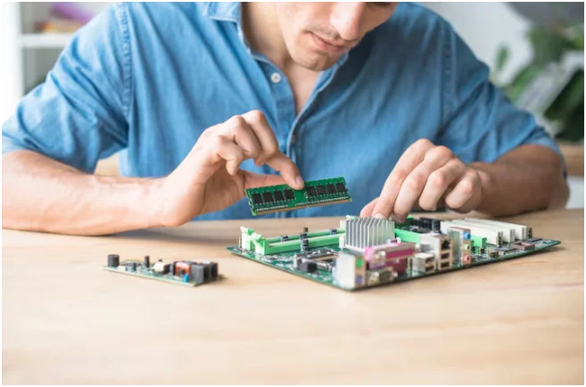
The Intricacies of PCB Design
Designing a PCB is both an art and a science, requiring a blend of electrical knowledge, software proficiency, and foresight into manufacturing constraints. The process begins with schematic capture, where engineers diagram the circuit using tools like Altium Designer or Eagle. This blueprint outlines component placements and connections, ensuring logical flow and minimal interference.
Next comes the layout phase, where the schematic translates into a physical board design. Key considerations include trace routing—pathways that carry signals—while avoiding crosstalk, electromagnetic interference (EMI), and thermal hotspots. Multi-layer PCBs, common in high-speed applications, stack insulating and conductive layers to maximize space and performance. For instance, a typical smartphone PCB might feature up to 12 layers to accommodate dense component integration.
Simulation tools play a pivotal role here, allowing designers to test for signal integrity, power distribution, and heat dissipation before prototyping. Software like Ansys or Cadence’s OrCAD enables virtual modeling, reducing costly revisions. Once designed, the board undergoes design rule checks (DRC) to verify compliance with manufacturing standards, such as minimum trace widths and clearances.
In practice, effective PCB design minimizes costs and enhances reliability. For example, optimizing component placement can reduce board size, which is crucial in space-constrained devices. Brands like Apple incorporate advanced PCB designs in their iPhones, using high-density interconnect (HDI) technology for slimmer profiles and faster data transfer. This meticulous process ensures that the final product not only works but thrives in real-world conditions.
Factors Influencing PCB Costs
Cost is a critical factor in PCB production, influenced by design complexity, materials, and volume. Basic single-layer PCBs for simple projects might cost as little as a few dollars per unit, while advanced multi-layer boards for aerospace applications can run into hundreds or thousands.
Material choice is a primary driver: Standard FR-4 substrates are economical, but high-frequency applications demand pricier options like Rogers laminates for better signal performance. Layer count escalates costs exponentially—each additional layer requires more fabrication steps, including drilling, plating, and lamination. For high-volume runs, economies of scale kick in, dropping per-unit prices significantly.
Manufacturing processes also impact expenses. Surface-mount technology (SMT) assembly is faster and cheaper than through-hole methods for dense boards. Additional features like gold plating for corrosion resistance or impedance control for high-speed signals add premiums. Prototyping incurs higher costs due to setup fees, but tools like rapid PCB services from providers such as JLCPCB or PCBWay help mitigate this by offering quick-turn options.
Design optimization can slash costs: Simplifying layouts reduces material waste and fabrication time. In automotive electronics, for instance, Tesla optimizes PCB costs by standardizing designs across models, balancing performance with affordability. Ultimately, understanding these factors allows engineers to make informed trade-offs, ensuring projects stay within budget without compromising quality.
Modern Uses of PCBs in Diverse Industries
The versatility of PCBs has propelled them into myriad applications, far beyond traditional computing. In consumer electronics, they power everything from laptops to smartwatches. Samsung’s Galaxy series, for example, relies on flexible PCBs to enable foldable screens, blending durability with innovation.
The automotive sector has embraced PCBs for advanced driver-assistance systems (ADAS) and electric vehicles. In Tesla’s vehicles, multi-layer PCBs manage battery systems and autonomous features, ensuring real-time data processing and safety. Medical devices, too, benefit: Pacemakers and imaging equipment use compact, biocompatible PCBs for reliable operation in life-critical scenarios.
Aerospace and defense demand rugged PCBs that withstand extreme conditions, such as vibration and radiation. NASA’s rovers incorporate specialized boards for space exploration. In renewable energy, PCBs in solar inverters and wind turbine controls optimize power conversion efficiency.
Emerging fields like IoT and 5G amplify PCB importance. Edge computing devices require high-speed, low-power boards to handle data deluge. As sustainability gains traction, eco-friendly PCBs using recyclable materials are on the rise, reducing electronic waste. These modern uses underscore PCBs’ role in driving technological progress across sectors.
Conclusion
From its humble origins to its pivotal role in cutting-edge tech, the Printed Circuit Board remains a cornerstone of electronics. By grasping the PCB full form, mastering design principles, navigating costs, and exploring its applications, we gain a deeper appreciation for the invisible infrastructure powering our world. As industries evolve, PCBs will continue adapting, fostering innovations that shape tomorrow. Whether you’re designing the next big gadget or simply using one, remember: behind every electronic marvel is a well-crafted PCB.

How Much Do Agencies Charge for Website Design? A Complete Guide for Businesses

From Personal Experience: Why a Specialized Estate Planning Attorney Can Change Everything

Why Simple Swaps Matter: Rethinking Everyday Bathroom Essentials